This is your first real complicated project in Verilog, so let’s really dive in. We are going to cover Continuous Assignment and Structural Verilog as opposed to Procedural Assignment and Behavioral Verilog. Those concepts will come later in this lab.
As such, let’s start with the two major concepts of Continuous Assignment and Structural Verilog, as they are foundational concepts upon which this lab is based. Thankfully, it’s in the name! If only it were that easy…
Basic Verilog Operators
Here’s the basic verilog operations:
| Operation | Verilog Syntax |
|---|---|
Single NOT |
Y = ~A |
Bitwise OR |
Y = A | B |
Bitwise AND |
Y = A & B |
Bitwise XOR |
Y = A ^ B |
Bitwise NOR |
Y = ~(A | B) |
Bitwise NAND |
Y = ~(A & B) |
Bitwise XNOR |
Y = ~(A ^ B) |
For these first labs, we will be dealing almost exclusively with wire
type structures. To build up a structural assignment, we need to use the
assign keyword. This will generally be the primary keyword you use.
Type assign <net> = <expression>; for each of the various structural
components of your circuit. Things declared as input or output
without any other specifiers are by default wire data types.
Using last lab’s tables, we know we can combine & (AND), | (OR), ^
(X-OR), and ~ (NOT) to build up our equations. The order of precedence
is… complicated – so just
use parens to force the order when you’re unsure. This generally makes
things easier to read at any rate.
Verilog Modules
Every Verilog file *.v must contain one or more verilog Modules. These
are discrete functional chunks of Verilog code that declare their
inputs, outputs, and the operations therein. Let’s look at an example:
module your_first_module(
    input A, // Single bit input -- END EACH LINE with a comma...
    input [5:0] B, // Six bit wide input
    output C, Another, // two single bit outputs (can be done for input too)
    output BitFour, // We can do any name for our outputs
                    // as long as it doesn't have whitespace in it
    output [5:0] D // Six bit wide ouput... without a comma
    // DO NOT PUT A COMMA AFTER THE LAST LIST ENTRY
); // Note this end paren with a semicolon

    assign C = A; // End each assignment with a semicolon

    wire invertC; // Declare local wires.
                  // These are neither inputs or outputs
                  // but can be used locally to hold values

    assign invertC = ~C; // And can be assigned to regularly
    assign Another = invertC; // And used as if they were regular values

    assign D = B; // When vectors match in size,
                  // they can just be directly assigned

    assign BitFour = B[4]; // Or decomposed for single elements

endmodule // No semicolon here for....... reasons
Modules are really cool, because when you have their input output declaration, you can use them as black boxes in other modules, composing higher level functionality out of small blocks:
module invert_input(
    input A,
    output NotA
);

    assign NotA = ~A;

endmodule

module top(
    input [1:0] sw,
    output [2:0] led
);

    // We can even have more than one of the same module!
    invert_input first( // Instantiate an invert_input named first
        .A(sw[0]), // Hook up its A to sw[0]
        .NotA(led[0]) // and its B to led[0]
    );

    invert_input first( // Instantiate an invert_input named second
        .A(sw[1]), // Hook up its A to sw[1]
        .NotA(led[1]) // and its B to led[1]
    );

    // And to use a signal between them, if required:
    wire inverted;
    invert_input contrived(
        .A(sw[0]),
        .NotA(inverted) // Hook up its output to our new wire instead
    );

    invert_input example(
        .A(inverted), // Use the output from the previous instance
        .NotA(sw[2]) // and send it wherever you need
    );

    // ----------------------------------------------------------------

    // There are other ways to refer to connect outputs:
    // If we wanted a module that used NotA from first,
    // you could do the following

    invert_input from_another(
        .A(first.NotA),
        .NotA(led[2])
    );

    // In addition, we can actually just use the already existing
    // wire, led[0]! Keep in mind all inputs and outputs are wire
    // types

    invert_input from_another_again(
        .A(led[0]),
        .NotA(led[2])
    );

    // Finally, we can do it with a direct wire

    wire between;
    invert_input first (
        .A(sw[0]),
        .NotA(between)
    );
    assign led[0] = between;
    invert_input from_another_again_again (
        .A(between),
        .NotA(led[2])
    );

endmodule
Continuous Assignment
This will likely be the stickiest point for many of you coming from
regular programming languages like C, Python, Java, etc. Verilog is
not procedural, (yes, even when using procedural assignment). There’s
no order of execution, there’s no entry point, there’s no main.
Verilog is a language designed and used to describe and construct
physical electrical circuits. As such, it does not behave like a
traditional programming language.
So, what do I mean by this? A way to think of it is that Verilog code effectively executes all at once, but really if you can envision it in your mind’s eye as if you are constructing a circuit and connecting wires, then you will be more successful. Let’s look at an example to help drive this home.
module demo1(
    input B, D, // Declare inputs
    output A, C // Declare outputs
);

    // Content of module
    assign C = ~A;
    assign A = ~B & D;

endmodule
This, in a traditional programming language, would likely result in a runtime or compilation error, as we are using A before we define it in our statement for C. But, in reality, this Verilog is simply describing this circuit:
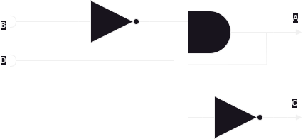
As you can see, there is no order to any of this. We tell the system that A is composed of B and D, then C is composed of A. We have connected these things together with wires. Where you put the various chunks in physical space doesn’t really matter. What we have area set of virtual wires (or, you may hear them called nets or something similar) that plug into structural chunks (OOH FORESHADOWING!). You’re not describing a process with Verilog, but the Structure of a physical thing.
This will be a major shift in thinking for many of you. The things you write here will seem to behave very strangely until you get used to thinking about it all happening at once.
Referring back to the lab
We know our final design needs three main chunks:
-
Circuit A
-
Circuit B
-
Top level file connecting the circuits to each other and to the switches
These are each in circuit_a.v, circuit_b.v, and top.v. Each of
those files will have a single module declaration in it called circuit_a,
circuit_b, and top respectively. We can reference these by those
names in the top.v file to create or instantiate those modules
over and over by different names, and wire them up to each other, or top
level inputs and outputs.
As a start, let’s go ahead and map in all of the I/O we decided on into
our top.v file. We will need these inputs and outputs to match the
names in our constraints file so that the place and route steps of
synthesis will know how to wire things up. In addition, our constraints
treat everything as a vector, or a bus of signals. In our I/O table, we
can see we uses switches 0 through 6 (inclusive) and LEDs 0 through 1
(inclusive). So, we will put those signals in MSB:LSB vectors:
module top(
    input [6:0]sw,
    output [1:0]led
);

endmodule
That covers our ports and their names. These will now map to the uncomment lines
in our constraints file to allow the synthesizer to place and route our design
to actual hardware. In addition, this gives us wire type elements to use in
our module. Let’s stick in the circuit_a module as an example:
module top(
    input [6:0]sw,
    output [1:0]led
);
    circuit_a a_inst(
        .A(sw[0]),
        .B(sw[1]),
        .C(sw[2])
        .D(sw[3])
        .Y(led[0])
    );
endmodule
In the above Verilog block, we’ve created an instance of circuit_a from
circuit_a.v called a_inst. Then, in the parentheses that follow, we wire up
the appropriate signals. For our design, as specified in the I/O table, we hook
up the signals A-D to sw[0] through sw[3], and the `Y signal to led[0].
Essentially, we directly translate our I/O table into Verilog.
Keep in mind how you might use a wire as we learned in the sections above to
connect between Circuit A and Circuit B. You would instantiate a Circuit B in
much the same way as shown above, but make sure that its A signal gets the
value from Y in Circuit A.
Something to Excite You
And, mind you, physical it actually will be! Here is the part where I
try to impress on you just how mind blowingly cool this technology is
that you have at your fingertips. Let’s launch Vivado and build our
circuit in reality. Create an empty project and add a single design
source we shall call top.v. Put the content of demo1 in this file,
then add the following piece of code:
module top(
    input [1:0] sw,
    output [1:0] led
);
    // This is an instantiation, not a function call
    // Think of it like plugging in a circuit to a breadboard
    demo1 uut(
        .B(sw[0]),
        .D(sw[1]),
        .A(led[0]),
        .C(led[1])
    );

endmodule
Alternatively, add the existing source demo_top.v to your project.
Then, load in the demo_constraints.xdc file into Vivado. When you are
done with this, hit the Generate Bitstream button and launch the
runs as it asks. When it finishes, select the Open Implemented
Design and hit OK.
It’ll pop up with a device view, like seen below:
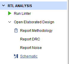
We will come back to this. First, in the panel on the left, hit the drop down next to Open Elaborated Design and click Schematic from there.
It will ask you if you want to close the other view first, hit Yes. You will now be presented with something that looks like this:
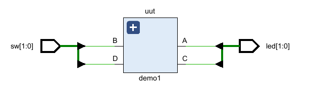
Click the + button in the top left corner. This will expand the schematic out to something like what you see below:
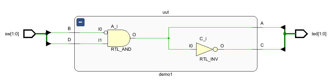
Hey! That looks an awful lot like my silly drawing up above. The tooling within Verilog translated our Verilog code into the virtual representation of a physical circuit. You can even see the little inverters and the AND gate exactly where we would expect to see them. But we can go deeper
Next, in the panel on the left, hit the drop down next to Open Synthesized Design, then click Schematic from there and open the synthesized design:
Another block diagram appears – similar to what we saw before, but there’s a few notable differences that are important to talk about here. Let’s look at the design here:
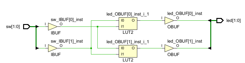
Even though it looks really similar, we can no longer see the clear AND gate and inverter that we saw above! What gives? During this step of the RTL compilation process, we have mapped the design onto the resources available for the FPGA we are targeting. Remember when you selected the Basys3 board as the design target for this project? That means we have actually specified an exact chip (the one on the board) and that allows Vivado to know exactly what and where everything on the board is.
So what we are seeing in this schematic is exactly the hardware pieces that we are recruiting to achieve our simple design. The IBUF and OBUF components are input and output buffers, and are outside the scope of this class, but you can read about them here. Then, there are two LUT instances – LUT meaning Look Up Table. This is how FPGAs actually work, it’s the secret sauce, the man behind the curtain.
Select one of the two LUTs. In the cell properties window in the bottom left of the Synthesized Design view, select Truth Table. Something like this should appear:
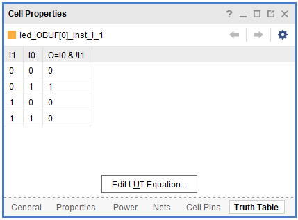
You can select and compare the two LUTs and see that each is implementing the exact required logic to make A and C happen as specified by our design.
Finally, we can go back to the implemented design. Open that, and keep
the device view open, the one we saw at the very beginning. if you look
at the top left panel, you should see a drop down for Nets, open that,
open led_OBUF, and select led_OBUF[0], then click the Auto-fit
selection option:
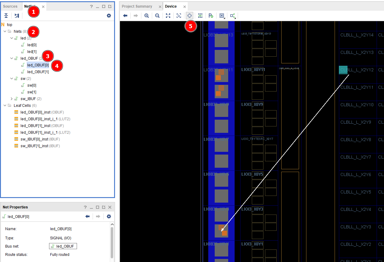
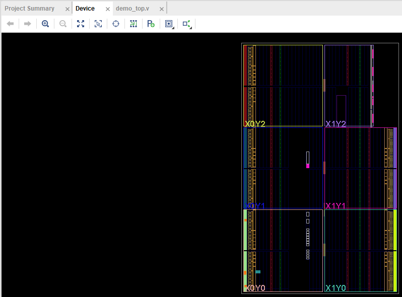
This has now focused our view of the FPGA in on our selected OBUF. What
we are seeing here is the exact physical layout of the piece of silicon
that is the FPGA on the Basys3 board. Highlighted are the exact chunks
of the FPGA that our RTL will be hooking together and loading equations
into in order to achieve the structure we designed in our top.v. Click
around this for a while and examine how each piece connects to each
other. You are in complete control of this hardware. It can do
anything and be anything. If you ask me, these are probably the single
coolest things mankind has ever created.