Introduction
In this week’s lab, we will investigate more advanced combinatorial logic equations and circuits. Now that you have the beginnings of understanding when it comes to Verilog, we can help you learn more in depth on the usage of verilog and digital logic.
One of the defining characteristics of combinatorial logic is to be able to develop subsystems and click them together like Lego. If each module declares its inputs and outputs, you can mix and match them together to build up more and more complex functionality out of these building blocks. To complete this lab, you will do just this, combining all the functional blocks you have built into one larger system.
To do this, I will introduce the concept of top level RTL blocks.
You can think of these like the main function in other programming
languages, it’s the entry point, as such even though there is no
execution sequence like in software programming, where one instruction
executes before another. The top level file will always combine all
functional blocks in a design and map them to the hardware.
BEFORE YOU CONTINUE: Please read how to verilog to learn about syntax, top level modules, and general Verilog guidance.
Part 1: Circuit A
Given the following truth table:
| A | B | C | D | Y |
|---|---|---|---|---|
0 |
0 |
0 |
0 |
0 |
0 |
0 |
0 |
1 |
1 |
0 |
0 |
1 |
0 |
0 |
0 |
0 |
1 |
1 |
1 |
0 |
1 |
0 |
0 |
0 |
0 |
1 |
0 |
1 |
1 |
0 |
1 |
1 |
0 |
0 |
0 |
1 |
1 |
1 |
1 |
1 |
0 |
0 |
0 |
0 |
1 |
0 |
0 |
1 |
0 |
1 |
0 |
1 |
0 |
0 |
1 |
0 |
1 |
1 |
0 |
1 |
1 |
0 |
0 |
0 |
1 |
1 |
0 |
1 |
0 |
1 |
1 |
1 |
0 |
0 |
1 |
1 |
1 |
1 |
0 |
Implement the circuit using Maxterms. Place the equation in the file called
circuit_a.v.
Part 2: Circuit B
Given the following truth table:
| A | B | C | D | Y |
|---|---|---|---|---|
0 |
0 |
0 |
0 |
1 |
0 |
0 |
0 |
1 |
0 |
0 |
0 |
1 |
0 |
0 |
0 |
0 |
1 |
1 |
0 |
0 |
1 |
0 |
0 |
1 |
0 |
1 |
0 |
1 |
0 |
0 |
1 |
1 |
0 |
1 |
0 |
1 |
1 |
1 |
0 |
1 |
0 |
0 |
0 |
1 |
1 |
0 |
0 |
1 |
0 |
1 |
0 |
1 |
0 |
0 |
1 |
0 |
1 |
1 |
0 |
1 |
1 |
0 |
0 |
1 |
1 |
1 |
0 |
1 |
1 |
1 |
1 |
1 |
0 |
1 |
1 |
1 |
1 |
1 |
1 |
Implement the circuit using Minterms. Place the equation in the file called
circuit_b.v.
Part 3: Connecting the Circuits
The next step in this lab is to connect circuit A to circuit B. In our case, we are saying that input A of circuit B is actually the output of circuit A. In short, it looks like this:
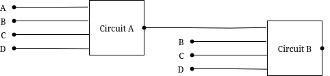
This gives us an IO table that looks something like this:
IO Table
| Pin | Purpose | Direction |
|---|---|---|
sw[0] |
Circuit A: Input A |
IN |
sw[1] |
Circuit A: Input B |
IN |
sw[2] |
Circuit A: Input C |
IN |
sw[3] |
Circuit A: Input D |
IN |
sw[4] |
Circuit B: Input B |
IN |
sw[5] |
Circuit B: Input C |
IN |
sw[6] |
Circuit B: Input D |
IN |
led[0] |
Circuit A: Output |
OUT |
led[1] |
Circuit B: Output |
OUT |
Notice how Circuit B has no Input A, that’s because we are using the output of
Circuit A as the first input of Circuit B. Implement this connection in the file
top.v.
Notice how A, B, C, and D of each circuit only gets meaning when we assign them by instantiating an instance of each module. This means several very cool things:
-
We can reuse these in future designs
-
They can fit on any FPGA as long as we can map the inputs
-
We can instantiate many of each design, giving different switches and LEDs to each as we see fit
Part 4: Constraining our design
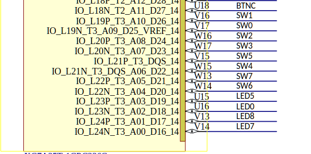
Each pin on the FPGA has a name the FPGA understands. In the case of the Basys3 board designed by digilent, that means the thing we know as SW0 is connected to the FPGA pin V17. This was decided by the engineers who did the hardware engineering and board layout for the Basys3.
So, our pin-to-function mapping has been decided by Digilent. How do we
tell Vivado that we mean V17 when we say SW0? Constraints. Open up the
included constraints.xdc file. This was provided for you in the previous
lab, but you won’t get so lucky twice. This file is directly taken from
Digilent’s own github repo, where they publish the default mappings for
all of their boards,
here.
What does this file actually say and mean? Let’s look at one line here:
#set_property -dict { PACKAGE_PIN V17 IOSTANDARD LVCMOS33 } [get_ports {sw[0]}]
It’s most simply read right to left. get_ports will pull a name from
your top level RTL file (in our case, top.v) and then operate on it.
We then call set_property on that pin, passing in a dictionary
(key/value pairs) of properties:
-
PACKAGE_PIN V17- This sets thePACKAGE_PIN, or the physical location ofsw[0]to V17. -
IOSTANDARD LVCMOS33- This sets theIOSTANDARD, or the voltage level standard of the pin toLVCMOS33. Read more about voltage standards here. Effectively, we are declaring this to be a 3.3V logic level pin.
There are a ton of other things that can be done in these statements, but for
the most part, during this lab, you will be simply uncommenting the lines that
correspond to your design and making sure the names match to your top level
file. Go through the constraints.xdc file and uncomment all the I/O pins we
need, based on the IO table in the section above.
Lab Deliverables
Summary of IO Table
| Pin | Purpose | Direction |
|---|---|---|
sw[0] |
Circuit A: Input A |
IN |
sw[1] |
Circuit A: Input B |
IN |
sw[2] |
Circuit A: Input C |
IN |
sw[3] |
Circuit A: Input D |
IN |
sw[4] |
Circuit B: Input B |
IN |
sw[5] |
Circuit B: Input C |
IN |
sw[6] |
Circuit B: Input D |
IN |
led[0] |
Circuit A: Output |
OUT |
led[1] |
Circuit B: Output |
OUT |
Required modules to implement
-
Implemented equation for Circuit A in
circuit_a.vdescribed in this section -
Implemented equation for Circuit b in
circuit_b.vdescribed in this section -
Filled out
constraints.xdcas described in this section -
Combine the two circuits above into a
top.vusing the IO table above and described in here. -
Demonstrate the combined design to TA or lab professor